Terahertz and Nanotechnology
|
Stefan Bengtsson Department of Microtechnology and Nanoscience, Chalmers University of Technology |
|
Many applications in electronics, photonics, materials and life sciences are rapidly evolving based on progress in nanotechnology. A good example is the development in the THz or sub-millimetre-wave field covering generation and detection of electromagnetic radiation in the frequency range from 300 GHz to 10 THz. The “gap” between microwave applications and photonics is closing with the progress of development of new source and detector devices, to a large extent propelled by nanotechnology development. With energy levels in the 1-40 meV range, terahertz interactions with matter involve intramolecular, rather than atomic transitions. This gives rise to several imaging and spectroscopy applications that are unique to this particular region of the electromagnetic spectrum. When room temperature robust component techniques are available the field of terahertz technology will enter a new phase. For instance, sub-millimetre wave imaging systems for a range of safety and security applications will be feasible. They are based on the ability of terahertz waves to penetrate fog and rain and image inside most dielectric materials, which may be opaque to visible light and have low contrast for X-Rays. Another example is a number of applications in biology and medicine based on the fact that the photon energy span of the THz-region is consistent with molecular vibrational modes in liquids and solids and hence enables to a certain degree “THz-fingerprinting”. Chalmers has a long history in development of sensitive high frequency detectors for radio astronomy linked to the Onsala Space Observatory, a national facility hosted by Chalmers. Over the last decades many research highlights have been presented, for instance a state-of-the-art low noise hot electron bolometer (HEB) for detection at THz frequencies and a first report on a fully integrated superconducting circuit above 300 GHz. Recently, Chalmers delivered an HEB system to the European Space Agency (ESA) for use in the satellite based Herschel telescope. In the semiconductor area several internationally recognized research results have been produced based on a number of device technologies, such as HEMTs, HBVs, RTDs, UTC-PDs, TEDs and Schottkys.
Today, THz technology work is made on both semiconducting and superconducting technologies aiming at for instance multipliers, mixers, photomixer sources for applications in imaging, safety, security and information technology. New material systems (i.e. carbon based) are employed for device manufacturing. The simultaneous build up and consolidation of activities in nanophotonics, biological physics, nanobio technology and systems biology at Chalmers opens perspectives for the coming years.
The presentation will overview the field of nanotechnology for THz technology and focus on recent research accomplishments in nanotechnology and THz technology at Chalmers of relevance for the development of new THz sources and detectors aiming at applications to information technology, safety and security, radio astronomy and bio sciences. The THz activities fit well into a strategic focus of the university. Chalmers University of Technology as well as the owner of the university, Chalmers Foundation, have made and are presently making large strategic investments in the fields of nanoscience/ nanotechnology and bio science.
|
Stefan Bengtsson
Chalmers University of Technology
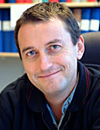
Stefan Bengtsson was born in Göteborg, Sweden, 27th September 1961. He received his MSc in Engineering Physics 1985 and his PhD in Solid State Electronics 1992 from Chalmers University of Technology. In 200-2001 he spent a period as visiting professor at ENSERG, Institute National Polytechnique Grenoble, France. Since February 2007 he is Executive Vice President of Chalmers.
Stefan Bengtsson’s research field is in silicon devices and structures. During the last years his efforts in integration of other materials and device technologies to the silicon CMOS platform has become a major part of the research activities. In the initial part he worked on semiconductor wafer bonding, a technique of bringing materials together and thereby building device structures and SOI materials. In the activity directed towards SOI materials and technology the focus has been at the development of advanced electronic materials such as silicon-on-diamond and silicon-on-aluminium nitride materials as well as at depleted RF substrates. In the field of MOS devices his major interest has been on gate dielectrics for future MOS transistors. The activity included low temperature oxides for silicon or silicon/germanium devices and recently different metal oxides for silicon dioxide replacement. Since 1999 Stefan Bengtsson has begun searching cross-disciplinary collaborations aiming at researching various approaches for “More-than-Moore”. As a consequence his recent project portfolio contains activities aiming at integrating silicon based devices, including CMOS as well as innovative silicon nanogaps, with other technologies, such as molecules or carbon nanotubes to extend the possibilities beyond what can be offered by silicon-only solutions. A major part of this activity is investigations of CMOS compatible process schemes to realize carbon nanotube-based nano-electro-mechanical systems (NEMS) on silicon.
Stefan Bengtsson is principal investigator in several national as well as European grants. He is coordinator of the EU FP6 Transnational access project MC2ACCESS, opening up the cleanroom facility at Chalmers for European researchers. Stefan Bengtsson has graduated around 10 PhD students and he has published more than 100 peer reviewed articles and conference papers. He is serving as member of around organizing and technical program committees of international conferences in Europe, the US, Asia and South America. He is member of the scientific committee of ESSONN, the European School of Nanosciences and Nanotechnology (www.esonn.inpg.fr), and is member of the Education and Training Coordination Board as well as the Scientific Community Council of the European Technology Platform “ENIAC” (www.eniac.eu). He presently serves on the board of “Chalmers Industriteknik” and of “Innovationsbron Väst”. In 1992 he received the SAAB-Scania Award for the PhD thesis and in 1998 he received the best Teacher Award of the Computer Science Program at Chalmers for lecturing the basic course in semiconductor devices.
|
| >> Program |